hankyoreh
Links to other country sites 다른 나라 사이트 링크
Intel to romp home in race to 1 nm, looks to overtake Samsung by 2030
Despite being a latecomer to the semiconductor foundry industry, Intel revealed that it will be the first to introduce a 1.4-nanometer process, which it’s dubbed Intel 14A. By overtaking TSMC and Samsung Electronics, the top two companies in the field, the company has added fuel to the flames of the competition to create 1-nanometer chips.
In addition, Intel also vowed to surpass Samsung Electronics, the No. 2 in the industry, by 2030 through the creation of a service that will allow advanced packaging and testing of semiconductor chips separately from assembly.
Many observers are waiting to see whether Intel’s reentry into the industry will prove to be a game changer that’ll shake up the US$140 billion global foundry market.
Intel held its first “Direct Connect” foundry forum on Wednesday (local time) in San Jose, California. There it announced its roadmap to move beyond the 1.8-nm process, Intel 18A, which it plans to introduce in 2025, and launch products with 1.4-nm chips in 2027 (Intel 14A-E, 1.4 Nano Gen 2)
This marks the first time Intel announced plans to move to a 1.4-nanometer process. Intel’s 1-nanometer process plan alone is about a year ahead of Samsung Electronics and TSMC, which are considered to have far more advanced technology.
Being the first to market advanced processes is part of a latecomer strategy to show off technology and attract customers. Intel announced its reentry into the foundry business in early 2021.
Intel was the first in the industry to receive high numerical aperture extreme ultraviolet (high-NA EUV) lithography systems from Dutch semiconductor equipment maker ASML in late 2023, and will utilize those systems in its Oregon plant.
These systems, which achieve finer wavelengths, are said to be essential for breaking through the highest process level of 2 nm. Each machine is estimated to cost more than 500 billion won, or around US$376 million.
However, the industry seems skeptical of Intel’s plans to produce products with 1-nm fabrication in less than five years, since the company struggled with sub-10-nm fabrication.
“There’s much to doubt about the stability of a plan for a company, that lacks experience in the mass production of semiconductor ultra-fine processes, to jump from 7 nm to 3 nm in such a short amount of time, and suddenly take a huge leap towards a 1-nm fabrication,” commented a semiconductor industry insider who wished to remain anonymous.
“It remains to be seen whether they will be able to do more than mere technology development and increase yields and make profit,” they added.
Intel is planning to increase cross-industry collaboration to bolster legacy process technologies as well as advanced technologies.
Taiwan’s UMC, which is strong in legacy process technology, will provide intellectual property, design assets, from its 12-nanometer and larger processes, while Intel will support its finFET— fin field-effect transistor — process technology.
The goal is to grow foundry influence in the medium to long term, given that half of industry frontrunner TSMC’s revenue comes from legacy processes.
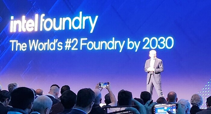
Intel said on Wednesday that it will create a new “systems foundry” that separates chip production from subsequent packaging (downstream processes such as chip placement and assembly) to “become the world’s second largest foundry by 2030.”
For example, by separating the many layers that had been conducted simultaneously in the existing foundry services, such as chip production, packaging and testing, it is possible to provide post-processing and testing services for chips from other manufacturers.
The strategy is designed to maximize Intel’s strengths in packaging and testing, as 3D printing and the ability to combine different chips into one will become increasingly important to efficiently keep up with the explosion of data in the era of artificial intelligence.
“This is creating an unprecedented opportunity for the world’s most innovative chip designers and for Intel Foundry, the world’s first systems foundry for the AI era. Together, we can create new markets and revolutionize how the world uses technology to improve people’s lives,” Intel CEO Pat Gelsinger announced at the forum.
Sam Altman, the CEO of OpenAI, also attended the forum and announced the company’s commitment to further collaboration with Intel on AI semiconductors.
The forum was also attended by US Treasury Secretary Gina Raimondo, Microsoft CEO Satya Nadella, and UK chip design firm Arm CEO Rene Haas.
By Ock Kee-won, staff reporter
Please direct questions or comments to [english@hani.co.kr]

Editorial・opinion
![[Column] Season 2 of special prosecutor probe may be coming to Korea soon](https://flexible.img.hani.co.kr/flexible/normal/500/300/imgdb/original/2024/0426/3317141030699447.jpg "[Column] Season 2 of special prosecutor probe may be coming to Korea soon") [Column] Season 2 of special prosecutor probe may be coming to Korea soon
[Column] Season 2 of special prosecutor probe may be coming to Korea soon![[Column] Park Geun-hye déjà vu in Yoon Suk-yeol](https://flexible.img.hani.co.kr/flexible/normal/500/300/imgdb/original/2024/0424/651713945113788.jpg "[Column] Park Geun-hye déjà vu in Yoon Suk-yeol") [Column] Park Geun-hye déjà vu in Yoon Suk-yeol
[Column] Park Geun-hye déjà vu in Yoon Suk-yeol- [Editorial] New weight of N. Korea’s nuclear threats makes dialogue all the more urgent
- [Guest essay] The real reason Korea’s new right wants to dub Rhee a founding father
- [Column] ‘Choson’: Is it time we start referring to N. Korea in its own terms?
- [Editorial] Japan’s rewriting of history with Korea has gone too far
- [Column] The president’s questionable capacity for dialogue
- [Column] Are chaebol firms just pizza pies for families to divvy up as they please?
- [Column] Has Korea, too, crossed the Rubicon on China?
- [Correspondent’s column] In Japan’s alliance with US, echoes of its past alliances with UK
Most viewed articles
- 1‘We must say no’: Seoul defense chief on Korean, USFK involvement in hypothetical Taiwan crisis
- 2[Editorial] Korea’s surprise Q1 growth requires objective assessment, not blind fanfare
- 3[Column] Season 2 of special prosecutor probe may be coming to Korea soon
- 4Division commander ordered troops to enter raging flood waters before Marine died, survivor says
- 5Is Japan about to snatch control of Line messenger from Korea’s Naver?
- 6The dream K-drama boyfriend stealing hearts and screens in Japan
- 7[Column] ‘Choson’: Is it time we start referring to N. Korea in its own terms?
- 8No good, very bad game for Korea puts it out of Olympics for first time since 1988
- 9[Special report- Part III] Curses, verbal abuse, and impossible quotas
- 10S. Korea “monitoring developments” after report of secret Chinese police station in Seoul