hankyoreh
Links to other country sites 다른 나라 사이트 링크
Japan, China make strides in cutting-edge chipmaking tools, accelerating tech competition
As the competition to acquire advanced semiconductors becomes a core part of industry policies for countries around the world, the race has been heating up to acquire the next-generation lithography equipment essential for the advanced semiconductor production process.
The extreme ultraviolet (EUV) lithography equipment produced by the Dutch company ASML currently holds a monopoly on the market, while Japan and China are striving to make advanced semiconductor production equipment using new methods that sidestep patented EUV technology.
Analysts predicted that the question of whether they can commercialize this technology will have a bearing not only on semiconductor company competitiveness but also on the race between the US and China for technological dominance.
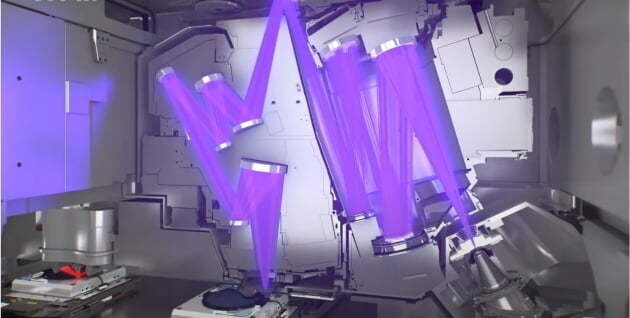
According to explanations Tuesday from semiconductor industry sources, Canon launched its FPA-1200NZ2C nanoimprint lithography equipment around mid-October. This equipment allows for the production of advanced semiconductors at scales below 5 nanometers (nm) without the use of EUV technology.
The technology, which skirts around ASML’s EUV lithography patents, has the added advantage of substantially reducing power costs, as it does not require a special light source like EUV.
Lithography is the part of the semiconductor production process that involves “printing” circuit diagrams onto wafers. Since semiconductor production competitiveness hinges on how precisely the circuit line widths can be drawn, the acquisition of lithography equipment capable of performing this precise work translates into competitiveness for semiconductor companies.
ASML is the only company in the world producing EUV lithography equipment, which is key to the production of advanced semiconductors at scales of 7 nm and under. One machine has an estimated cost of around US$200 million, with only around 60 of them produced per year.
While Canon has not yet reached the level of producing this EUV lithography equipment itself, its strategy is about targeting niche markets.
In a recent press interview, Canon CEO Fujio Mitarai said, “The price will have one digit less than ASML’s EUVs.”
“I don’t expect nano-imprint technology to overtake EUVs, but I’m confident this will create new opportunities and demand,” he added.
China has also made some notable movements. In a bid to overcome US regulations on equipment exporting, it is pushing to develop semiconductor production equipment using particle accelerators.
According to a report in Hong Kong’s South China Morning Post, the success of Tsinghua University researchers in a project using particle accelerators to create a laser source has led the Chinese government to pursue plans for creating a large-scale semiconductor lithography equipment factory based on this technology.
If this comes to pass, it opens the way for China to independently produce advanced semiconductors at the 2 nm level.
While the US has barred the transportation of EUV lithography equipment into China, China has been busy attempting to find workarounds. A report released Monday by the Korea Institute for International Economic Policy predicted that while Washington’s increased export control measures on chipmaking equipment and technology to China would pose major roadblocks for China’s manufacture of semiconductors, these controls would also serve as an impetus for Beijing to actively pursue equipment self-reliance, as demonstrated by the establishment of a fund to this end worth US$40 billion.
“There’s a possibility of mid- to long-term demand [for Canon’s equipment] particularly among small foundries that find it challenging to get their hands on pricey EUV equipment,” remarked a Korean semiconductor sector insider, who was reluctant to give their name. “It could be used as an alternative for circumventing US regulations in China, where ASML equipment can’t be imported.”
Baek Seung-hye, a researcher at Hana Securities, said that from January through August of this year, the proportion of domestically made equipment that won foundry equipment bids rose to 47% — more than twice the 20% that it was in 2021. “Home production of equipment has progressed rapidly, and with accumulated manufacturing experience, there’s a greater possibility that China could break the 7 nm or lower floor.”
By Ock Kee-won, staff reporter
Please direct questions or comments to [english@hani.co.kr]

Editorial・opinion
![[Editorial] Perilous stakes of Trump’s rhetoric around US troop pullout from Korea](https://flexible.img.hani.co.kr/flexible/normal/500/300/imgdb/original/2024/0509/221715238827911.jpg "[Editorial] Perilous stakes of Trump’s rhetoric around US troop pullout from Korea") [Editorial] Perilous stakes of Trump’s rhetoric around US troop pullout from Korea
[Editorial] Perilous stakes of Trump’s rhetoric around US troop pullout from Korea![[Guest essay] Preventing Korean Peninsula from becoming front line of new cold war](https://flexible.img.hani.co.kr/flexible/normal/500/300/imgdb/original/2024/0507/7217150679227807.jpg "[Guest essay] Preventing Korean Peninsula from becoming front line of new cold war") [Guest essay] Preventing Korean Peninsula from becoming front line of new cold war
[Guest essay] Preventing Korean Peninsula from becoming front line of new cold war- [Column] The state is back — but is it in business?
- [Column] Life on our Trisolaris
- [Editorial] Penalties for airing allegations against Korea’s first lady endanger free press
- [Editorial] Yoon must halt procurement of SM-3 interceptor missiles
- [Guest essay] Maybe Korea’s rapid population decline is an opportunity, not a crisis
- [Column] Can Yoon steer diplomacy with Russia, China back on track?
- [Column] Season 2 of special prosecutor probe may be coming to Korea soon
- [Column] Park Geun-hye déjà vu in Yoon Suk-yeol
Most viewed articles
- 1‘Free Palestine!’: Anti-war protest wave comes to Korean campuses
- 2[Editorial] Perilous stakes of Trump’s rhetoric around US troop pullout from Korea
- 3Behind-the-times gender change regulations leave trans Koreans in the lurch
- 4Nuclear South Korea? The hidden implication of hints at US troop withdrawal
- 5Korean president’s jailed mother-in-law approved for parole
- 6[Photo] ‘End the genocide in Gaza’: Students in Korea join global anti-war protest wave
- 7In Yoon’s Korea, a government ‘of, by and for prosecutors,’ says civic group
- 8Korea likely to shave off 1 trillion won from Indonesia’s KF-21 contribution price tag
- 9With Naver’s inside director at Line gone, buyout negotiations appear to be well underway
- 1060% of young Koreans see no need to have kids after marriage